Unit 6:BOOLEAN ALGEBRA AND LOGIC GATES
Key Unit Competency
By the end of this unit, you should be able to:
1. Identify different logic gates, theorems of boolean algebra and
evaluate boolean expressions.
2. Utilise laws of boolean algebra on boolean expressions and draw a
simple logic circuit using logic gates.Unit Outline
• Circuits and Logic gates.
• Logic gates.
• Truth tables
• Solving problems using logic circuits
• Boolean Algebra.
• Sum of Product (SOP) and Product of Sum (POS)Introduction
As you may be aware, most modern computers are digital and they use binary logic
to process data which is represented as a series of 0’s and 1’s. In this chapter, we start
by looking at simple logic circuits that form the fundamental building blocks of data
processing in computers. We then briefly look at boolean algebra and its connection
to logic reasoning.6.1 Circuits
Activity 6.1: Switching a torch on and off
Hold a torch. Switch it ON. After a while, switch it OFF. What do you think makes
the torch to give light when you move the switch to the ON position?Simplic circuits representing logic gates
Before we look at logic gates, let us try to represent basic logic operations using an
arrangement of switches that can control the states of a light bulb, either to go ON
or OFF. Figure 6.1 shows a normal simple electrical circuit: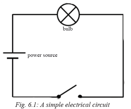
In Figure 6.1 above, when the switch is OPEN (state 0) the bulb is OFF (state 0) too.
When the switch is closed (state 1) then the bulb comes ON (state 1) too because
there is flow of electricity in the circuit.6.1.1 NOT circuit
Now study Figure 6.2 below. You will notice that it has a different arrangement. In
this circuit, when switch A is open, the bulb comes ON since there is a complete
flow of electrical current in the circuit. However, when A is closed, the bulb finds
itself in between two +ve opposing voltages that are equal to each other so it goes
OFF. Therefore, when the state of the switch is 1, that of the bulb is at 0. This is a
generally referred to as the inversion or NOT operation i.e. it inverts the input from
1 to 0 and vice versa.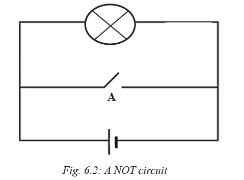
6.1.2 AND circuit
In Figure 6.3 below, both switch A AND B must be closed (in state 1) before the bulb can light. If either or both switches are open, the bulb is also OFF. This circuit represents the AND logic where all the switches must be closed in order to light the bulb.
6.1.3 OR Logic
Figure 6.4 below shows a circuit that represents the OR logic. In this case if either switch A OR B is closed, the bulb will light. The bulb will be off only if both switches A and B are open at the same time.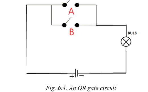
6.2 Logic gates
A logic gate is the basic building block of a digital circuit. A digital circuit is one that can only be in one of two states at any one time, either ON or OFF. An ON means there is high voltage in the circuit while an OFF means zero or no voltage in the circuit. It usually has an input side (with one, two or more inputs) and a single output. The input(s) can receive either ON or OFF signals usually represented by 1 or 0 then depending on the logic within the gate, the output can either be 1 (one) or 0 (zero). Although a single logic gate is simple, many of them are combined together into a complex maze to enable complex circuits which process data in the computer at the low level depending on the type of signals that are input.Basic logic gates
There are quite a number of different logic gates. However, the basic ones are shown
in table 6.1 below. Before discussing each one of them, take note of their names and
drawing. You should be able to identify and/or draw the representation of a particular
gate.
6.3 Truth tables
A truth table is a mathematical table used in boolean algebra or propositional logic to
compute the outcome of all possible combinations of input values i.e. it can be used
to tell whether an expression is valid for all legitimate input values. For example,
if the inputs A and B can take values 0 and 1; then possible combinations for inputs
(A,B) are {(0,0), ),(0,1), (1,0) and (1,1)}.
Assuming Q is the output, each logic gate gives different outputs based on the
combination of these values (see Figure 6.2).
The truth tables are important because they help us to know the output of each
individual gate given certain inputs hence we can use them to construct more complex
logic circuits that can solve real problems.
Given a particular truth table, it should be possible for you to know which logic gate
or combination of logic gates produced it. An increase in the number of logic gates
also expands the truth table.Truth tables for various logic gates
Based on the characteristics of individual logic gates discussed in Table 6.1, we can
be able to investigate the behaviour of each gate when a combination of inputs are
used. For the sake of simplicity, we look at gates that have only two inputs and one
output. We accomplish this by constructing truth tables. A truth table arranges all
possible input combinations and their relevant outputs (Figure 6.5). In this case, A
and B represent inputs to the logic gate while Q the output.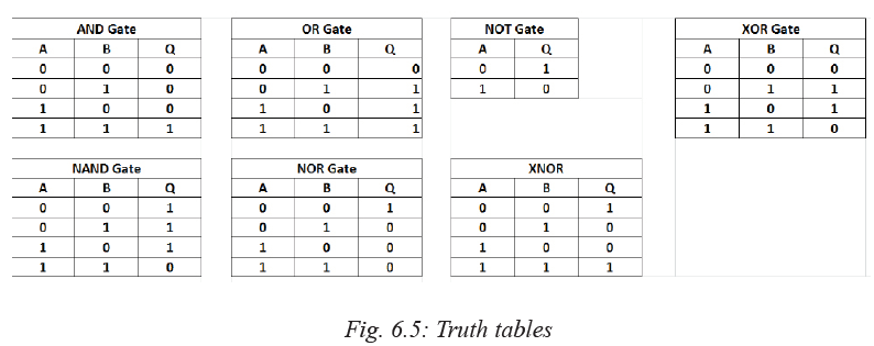
Activity 6.2: ICs and their internal logic gate structure
Groupwork:
The integrated circuits (ICs) that we have in our electronic devices like radios,
televisions, mobile phones, tablets and computers look like the pictures in Figure
6.6 (a). The internal structure of some of such ICs is shown in Figure 6.6(b)(i) and
(ii). Study them then answer the questions that follow: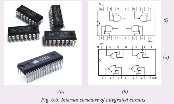
1. Identify the gates that are found in each of the ICs (i) and (ii) above.
2. In IC (i): If a high voltage signal is fed at pin 13 and a low voltage signal at pin 12, what will be the output at pin 11?
3. In IC (ii): If a low voltage signal is at pin 2 and 3, what will be the output at pin 1?Activity 6.3: Example of coming up with truth tables
Individual work:
Study the following logic circuit in Figure 6.7. Construct a truth table for the circuit.
Do not look at the provided solution first.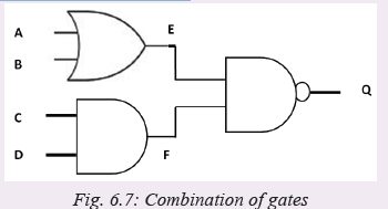
Solution: Notice that the logic circuit has four inputs. This expands the different input
combinations to 16 i.e: (A,B,C,D) = {(0000),(0001),(0010),(0011),(0100),(0101),(0
110),(0111),(1000),(1001),(1010),(1011),(1100),(1101),(1110),(1111)}.
How to work out the solution:
1. Start by looking at the inputs A and B. Remember that for an OR gate, if either
of them or both of them are 1 then the output E will be 1 otherwise it would be 0.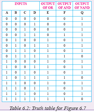
2. Move to the inputs C and D. Remember again that for an AND gate both inputs
need to be 1 in order for the output F to be 1 otherwise all other combinations
produce output F = 0.
3. Lastly, E and F are inputs to the NAND gate. For Q to be 0 then both E and F
must be 1 otherwise Q will be 1 in all other combinations. Therefore, the truth
table for the circuit in Fig. 6.7 is as shown in Table 6.2:Activity 6.4: Example of logic gate identification from given truth table
Pair Work:
Given the following truth tables (Table 6.3), draw and name the logic gate or combination of logic gates that can produce them. Assume A,B are inputs while Q is
the output. Try to answer before looking at the solution.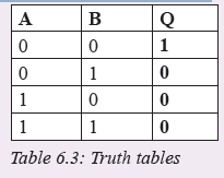
Solutions
(a) Looking at the truth table, the gate has two inputs. The output of the gate resembles
that one of an OR gate followed by a NOT gate. Hence, this is a NOR gate
(Figure 6.8).
6.4 Solving problems using logic circuits
Many problems in mathematics and computer science are solved through two valued
logic; every statement is either True or False (1 or 0). In life, problems are solved
by logically thinking through all possible courses of action and coming up with a
conclusion of the best way to solve the problem. In coming up with the solution, the
logician comes up with all valid arguments. Logical statements that describe problems
can therefore be solved using logical circuits or their equivalent truth tables.Activity 6.5: Example of using logic gates to construct a light switch
Think of a situation where you are requested to use the appropropriate logic gate(s) to construct a light switch i.e. when the switch is ON (True), the light is ON (True)
too; but when the switch is OFF (False), position of the light goes OFF (False) too.Solution
This is typically two NOT gates arranged one after the other. The truth table for the circuit will be as follows:
Activity 6.6: Solving real life problems
Groupwork:
In groups of four, try to find the solution to this problem. Do not look at the solution
provided first.
An alarm bell uses three sensors to determine whether it should sound or not. Two
sensors A and B are inside the room while C is hidden somewhere outside the room.
If either sensor A or B or both detect motion in the room and C never reported sensing
motion outside, then the system knows that there is an intruder. An ON signal is sent
to the bell and the bell rings loudly. Only authorised persons know where sensor C is
hidden outside the room. To safely enter the room, they have to follow a procedure i.e.
start by standing in front of C for the system to sense their presence before entering
the room. In that case all the sensors A, B and C will have detected the presence of
an authorised person, therefore, no signal will be sent to the alarm for it to ring. In
essence, as long as C detects motion, the alarm assumes that the person entering the
room is not an intruder. Draw a logic circuit that would represent this logic and do
a truth table for it.Solution
We have to start by reasoning based on the logic gates possible inputs and outputs.
Let us start by assuming the alarm has three inputs A, B and C. This means one of
the gates has one input - hence it must be a NOT gate! Let us make the following
assumptions when reasoning about the inputs A, B and C; and output X.
1. If a sensor senses motion then there is a 1 signal at the sensor. If there is no
motion, there is a 0 signal at the sensor.
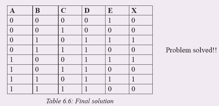
2. If X = 1, the alarm bell rings otherwise it does not ring.We start by constructing a truth table for the alarm circuit based on all possible
combinations of inputs A,B and C and expected output X as shown in Table 6.4 (a)
below. What we know is that for all instances where C = 1, then X = 0 i.e. when C
detects motion the alarm bell will not ring even if A and B detect motion.
We also know that where either A or B or both are 1(detect motion) and C = 0 then
X = 1. Of course where both A and B are 0 then X = 0 too since there is no intruder!
We can then fill in the gaps as shown in Table 6.4(b).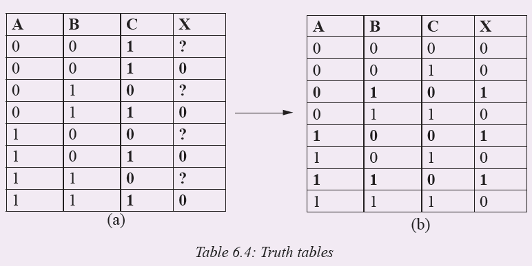
We can now construct a possible configuration of gates using a block diagram. All
we know for now is that one of the gates is a NOT gate. Let us conveniently assume
that the one on which sensor C is attached is our NOT gate. Looking at truth Table 6.4
(b) we can conclude that the output X of gate G2 depends on the output of the NOT
gate (E) together with that of G1 (D). Ideally, we keep remembering that whenever
E = 0, then X = 0.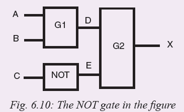
Let us expand the truth table (b) above, based on the knowledge we have to include
the outputs D and E. We can reason analytically to see whether we can finally find
out what type of logic gate G1 and G2 are: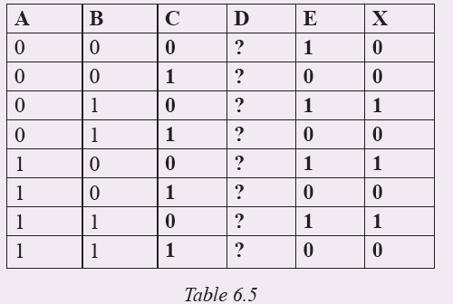
We take notice that every time either A or B or both are 1 then X = 1 only where E=1.
Therefore G2 behaves like an AND gate while G1 like an OR gate!! We sketch the
circuit (Figure 6.11) and verify it using a truth table:
Assessment Exercise 6.1
1. Define a logic gate.
2. What is a logic circuits truth table?3. Assuming that a NOT gate has an input 0, what will be its output?
4. Draw a NOT gate. Draw its truth table.
5. Assuming that an OR gate has one input at 1 and the other one at 0.
What will be its output?
6. Draw an OR gate. Draw its truth table.
7. What is the difference between an OR gate and a NOR gate.
8. Draw a NOR gate. Draw its truth table.
9. Differentiate between an AND and NAND gate.
10. Draw a NAND gate and its truth table.
11. Draw an XOR gate and its truth table.
12. Draw an XNOR gate and its truth table.
13. Develop truth tables for the following logic circuits (Fig. 6.12):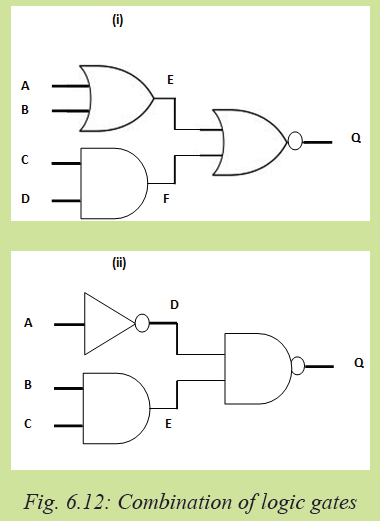
14. A company would like to come up with a logic circuit to monitor what is
happening in the boiler and get a warning well in advance before the situation
goes out of control. If the pressure (A), temperature (B) and humidity (C) are
low, then a signal is sent to the operator that there is something wrong with the
system. Similarly, if either pressure or temperature is high and the other low,
and the humidity is low, a signal will be sent to the operator. Develop a truth
table for this and draw the equivalent logic circuit.6.5 Boolean algebra
Boolean algebra was invented by George Boole in 1654. It can be used to automate the
manipulation of objects that control real life processes. This is because computers are
made up of digital switches that are either ON or OFF. Since the inputs and outcomes
of boolean algebra are either 1 or 0, it is a more natural way of representing digital
information or computing logic. The algebra is used to explain or solve problems
related to logic and digital circuits.6.5.1 Laws of boolean algebra
Boolean operations revolve around boolean operators. A boolean operator takes two
inputs of either 1 or 0 and output a single value also either 1 or 0.
There are several laws of boolean algebra. The most common operators that are used
to manipulate the various logic elements are the OR (+) and the AND(•) e.g.
A + B means A OR B.
A•B means A AND B or mostly just written as AB without the (•) symbol.
6.5.2 Boolean algebra simplification
Using the above laws, both simple and complicated boolean expressions and logic
circuits can be simplified and solved. Truth tables for the expressions are used to
come up with relevant solutions.
In normal algebra, it is possible to simplify complex expressions like 9x + 3y – 2x + 4y to their simplest forms like 7x + 7y i.e.
9x + 3y - 2x + 4y = 9x - 2x + 4y + 3y (simple rearrangement)
= 7x + 7y
Similarly, the boolean laws stated above can be used to simplify complex boolean
expressions. It is often the case that a complex boolean equation has to be simplified
into its simpler exact equivalent. This becomes very useful when one is designing
circuits and wants to minimise the number of gates needed to build the circuit. There
are two methods of simplifying boolean expressions:
1. Using truth tables.
2. Using boolean algebra which entails applying identities and De-Morgans law.
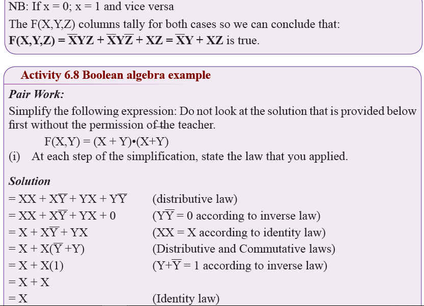
In this book, we shall rely on these laws as stated in section 6.5.1 and on truth tables.Activity 6.7: Boolean algebra example
Individual Work:
Study the example given below: Do the workings too as presented below.
Simplify the following boolean expression: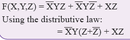

We can check using truth tables whether the complex form of the expression is
equivalent to the simplified form. The truth table for the complex form of the equation
is given below: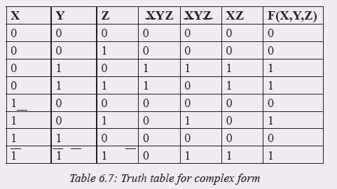
Let us look at row 1 to know how we are computing the values:
XYZ = 1•0•0 = 0 (remember for AND all have to be 1 to get a 1) i.e. on row
1 column 1, X; = on row 1 column 2 Y =0 and on row 1 column 3 Z = 0
XYZ = 1•0•1 = 0 (remember if A = 0 then A = 1)
XY = 0•0 = 0
F(X,Y,Z) = 0 + 0 + 0 = 0 (for row 1; remember OR gate)
F(X,Y,Z) = 0 + 1+ 0 = 1 (for row 3; remember OR gate if one of the
inputs is 1 the output is 1)
Let us now do the same with the simplified expression:
F(X,Y,Z) = XY + XZ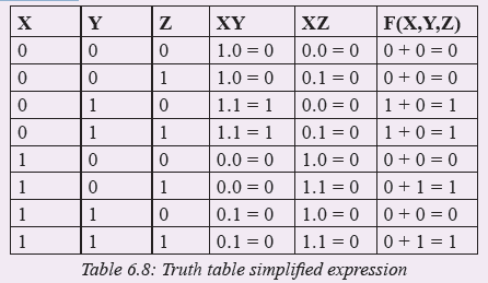
6.6 Sum of Product (SOP) and Product of Sum (POS)
Using truth tables to simplify boolean equations is good and straight forward.
However, when the logic circuits become more complex with more inputs, truth tables
become very cumbersome. It is desired therefore to find a better way of representing
logic in such scenarios. We use a standard form of boolean equations known as the
canonical form written in SOP or POS format. The SOP and POS equations help
a person to quickly derive solutions from a given logic table and come up with
equivalent logic circuits.6.6.1 Sum of products
We have so far seen that given a boolean value A, we assume that A = 1 and its
complement is A = 0. Conventionally, we can write a boolean expression which has
three variables in the following form:
F(A,B,C) = ABC + ABC + ABC
This kind of expression has three groups of the products of the variables A, B and
C (AND operations) which are summed together (ORed). We therefore call such an
expression a sum of products (SOP). Each term in the equation is called a minterme.g. ABC is one of the three minterms. However, note that the domain of three binary
variables is capable of generating eight different minterms but only three were chosen
for the above equation. We are going to see how such equations are generated from
truth tables.
In the SOP arrangement, the AND operations have precedence over the OR operations.
That means we first AND the terms in the minterms before we do the OR operations.
When representing minterms, we use a shorthand designation e.g. mx where x = 0,
1, 2 . . . n. For example, in the above domain where we have three binary variables
we can generate the following truth table.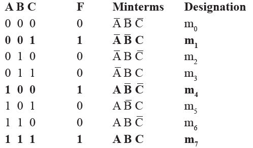
The minterms column represents the values of each variable A, B, C in the truth table
e.g. if A = 1 then we write it as A; If A = 0 we write it as A¯ in the minterm.
The values in the column F are user defined depending on how you wish your circuit
to behave i.e. in this case we want our circuit to give a 1 output if and only if:
¯A¯BC, AB¯C¯, ABC (i.e. check the rows where F = 1 as bolded in the table).
To create an equation that represents the required logic, we OR these minterms:
F(A,B,C) = ¯A¯BC + AB¯C¯ + ABC . . . . . . . . . . . . . . . . . . . . . . . . . . . . . . . (1)
This equation can be written using the designations as:
F = m1 + m4 + m7 as long as we have constructed the truth table
correctly and we know the variable combinations for each mx.NB: From the Equation 1 above, we can now be able to construct a logic circuit
that meets the conditions set by the equation. This method of coming up with logic
circuits is far much more easier. It means we can be able to work with a truth table
that has an arbitrary number of input variables and come up with simplified boolean
expressions which can then be used to construct logic circuits that meet the criteria set.Constructing an equivalent logic circuit
Let us now construct an equivalent logic circuit for Equation 1. We can quicklyunderstand each of the minterm combinations as follows:
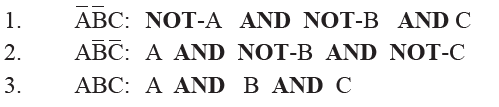
This means if you wish to create the logic circuit, you need three AND gates each
with three inputs for each of the variables in the minterms. The three outputs of the
AND gates then become inputs to a single OR gate of three inputs (remember you
have to OR the minterms). However, notice that we include a NOT gate on any input
that has a NOT operator in order to fulfill the required criteria (Figure 6.13).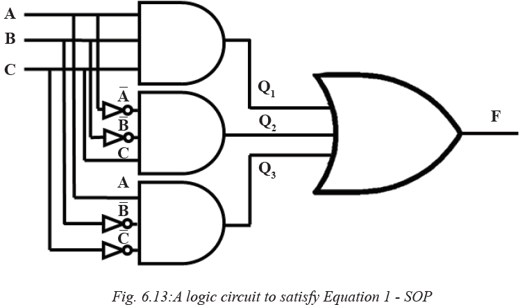
To verify whether the circuit meets the requirements of Equation 1, we can draw a
truth table to find out if we get a 1 output only at m1, m4 and m7 as is in Table .Activity 6.9: Verifying the logic circuit in Figure 6.13
Draw the truth table for the logic circuit in Figure 6.13. Discuss the outcome with
other students in the class as the teacher guides. Does your truth table have 1 outputs
in column F at m1, m4 and m7?6.6.2 Product of sums (POS)
The product of sums (POS) takes every combination of variables in the domain
and performs an OR operation. The OR operations are then ANDed. Each valid
combination is called a Maxterm and is designated as Mx where x = 1, 2, 3 . . . n.
The OR operations take precedence over the AND operations here. For example, if
we have a domain of three binary variables we can generate the following truth table: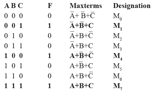
In this case, we can pick only those maxterms where the value of our function F = 1.
The maxterms can then be ANDed together as follows:
F(A,B,C) = (A¯+B¯+C)•(A+B¯+C¯)•(A+B+C) . . . . . . . . . . . . . . . . . . . . . . . . (2)
In order to design a logic circuit that will meet the criteria set by Equation 2, we
need three OR gates each with three inputs A, B and C. The output of the OR gates
can then be fed into an AND gate as shown in Figure 6.14.
Activity 6.10: Verifying the logic circuit in Figure 6.14
Draw the truth table for the logic circuit in Figure 6.14. Discuss the outcome with
other students in the class as the teacher guides. Does your truth table have 1 outputs
in column F at M1, M4 and M7?
Notice that as you work out the truth table for the logic circuit in Fig 6.14, all the
three OR gates need to give an output of 1 each i.e. Q1, Q2 and Q3 should all be equal
to 1 in order for the AND gate to give output of F = 1.Activity 6.11: Applying SOP and POS example
An air traffic control system controls the landing and taking off of aircrafts at the
airport. The system uses four input variables to determine whether an aircraft should
land or take off:
A: The direction and speed of the wind must be favourable.
B: The runway lights must be ON and clearly visible.
C: The runway must be clear and should not be slippery.
D: The pilot must be alert and in good health.
The system can give a green light for landing/take off in the following circumstances:
1. If B, C and D are okey. The pilot can be instructed on direction of landing/takeoff.
2. If all A,B,C,D are okey.
3. For all other combinations, the system will not allow landing/takeoff.
Use the sum of products strategy to come up with a logic circuit that can deliver the
right decisions to the air controller.
We start by constructing the truth table: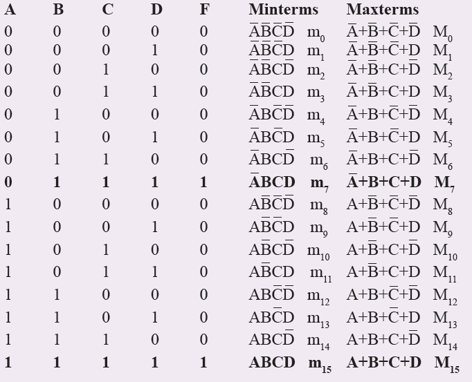
Notice that a four variable truth table is large. To satisfy the conditions 1,2 and 3
above, we set m7 and m15 as the only combination of the variables that will give us a
1 in the system i.e. the greenlight for a plane to land or take off. Following this, we
can then write the required equations as follows:

Equation 3 summarises the solution using the sum of products while Equation 4 uses the product of sums. After coming up with this equations, it is now possible to design logic circuits that would satisfy them. We shall develop the logic circuit for the sum of products. After that, we allow you to do the product of sums as an activity. Looking at Equation 3, we need two AND gates each with four inputs and one OR gate in order to come up with the equivalent logic circuit. The circuit is shown in
Figure 6.15.
Activity 6.12: POS logic circuit
Design the logic circuit for Equation 4 above. Share your solution with the rest of
the class.6.7 NAND and NOR as universal gates
Activity 6.13: NAND and NOR gates
Do some research about the NAND and NOR gates. Sketch them. Draw a two variable
truth table for each one of them. Present your work to the class.
Now look at Figure 6.13, 6.14 and 6.15. What gates have you used to create the logic
circuits with in all the examples and activities you have accomplished?We have discussed about different types of logic gates at the beginning of this chapter.
However, notice that the AND, NOT and OR gates are the most used when coming
up with logic circuits. Of course a combination of a NOT and AND gate creates a
NAND while that of a NOT and OR gates creates a NOR. Now NOR and NAND
gates have the unique property that any one of them can create and satisfy any logical
boolean expression if designed in a proper way. Hence we say that NAND and NOR
gates are universal gates.